
Impact of PCB Parasitic Capacitance on Switching Transients in Split-Phase Inverter Utilizing TO-247 SiC Devices
Abdul Basit Mirza, Yang Xie, Sama Salehi Vala and Fang Luo
2023 IEEE Energy Conversion Congress and Exposition (ECCE), 2023
Read Here
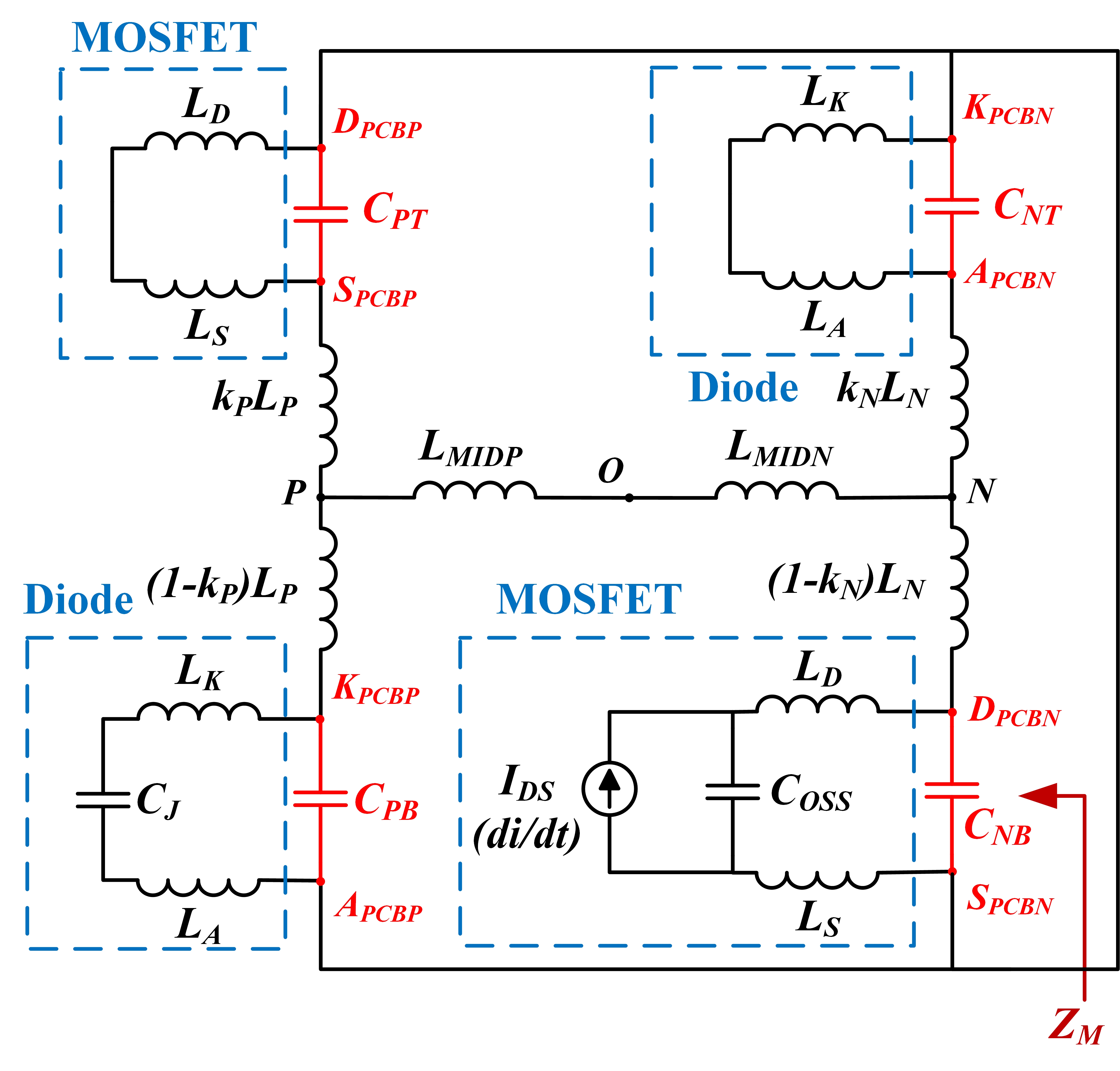
Abstract: The fast-switching capability of Wide Band Gap (WBG) devices has enabled high switching frequency and power density targets. However, fast switching implies high dv/dt and di/dt, imposing a constraint on the PCB power loop inductance in minimizing voltage overshoot during switching. Although vertical PCB power loop design is proven effective in achieving low loop inductance, the underlying PCB parasitic capacitance is increased. For a discrete device, the PCB parasitic capacitance is paralleled to the device’s output capacitance through the package lead inductance, altering the transient switching response, dv/dt and voltage overshoot. This paper analyzes the effect of PCB parasitic capacitance on switching transients in a two-level Split-Phase (2L-SP) inverter phase-leg with SiC devices in TO-247 package. The results show that PCB parasitic capacitance and package lead inductance impact the transient switching response and voltage overshoot, making the conventional second-order LC small-signal transient switching model inapplicable.
Recommended citation (BibTex):
@INPROCEEDINGS{MirzaPCB2023,
 author={Mirza, Abdul Basit and Xie, Yang and Vala, Sama Salehi and Luo, Fang},
 booktitle={2023 IEEE Energy Conversion Congress and Exposition (ECCE)},
 title={Impact of PCB Parasitic Capacitance on Switching Transients in Split-Phase Inverter Utilizing TO-247 SiC Devices},
 year={2023},
 volume={},
 number={},
 pages={5504-5509},
 doi={10.1109/ECCE53617.2023.10362372}
}